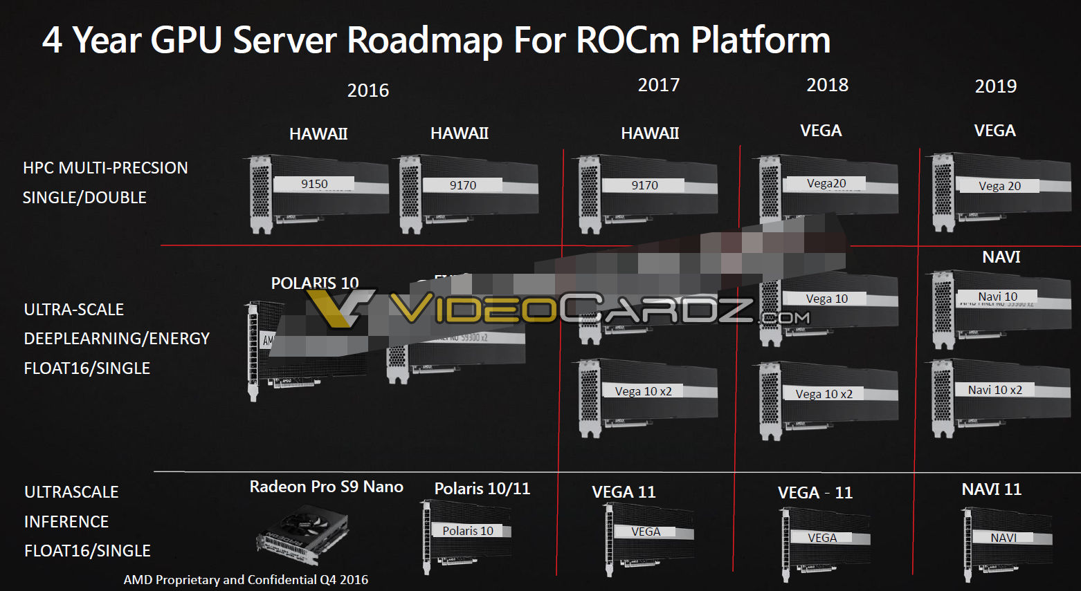
The slides we are sharing today are the same slides we described to you back in September (so they are not new). We are posting this because so far everything turned out to be (almost) correct.
Just a reminder, those slides are from internal presentation, they are not meant for public viewing, thus such design.
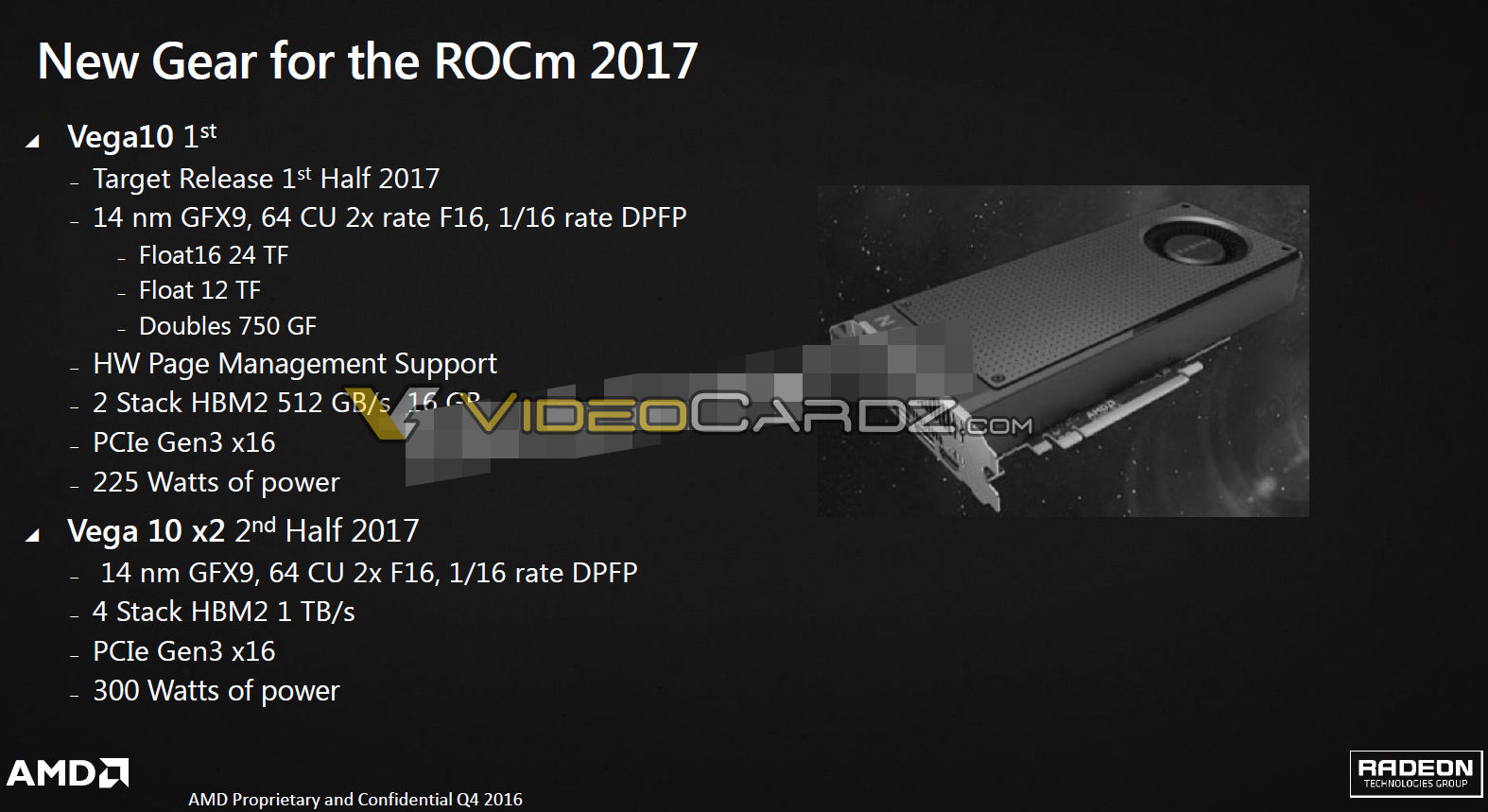
AMD VEGA 10
There are two cosmetic differences between this old slide and what we know today. The CU was renamed to NCU (Next-Generation Compute Unit). Also, the floating point performance increased from 12 to 12.5 TFLOPs in 32-bit operations. Notice that the slide also says 2 stack HBM2, confirmed by VEGA reveal just yesterday (partially the reason why I decided to post this today).
VEGA 10 will feature 14nm GFX9 architecture with 64 compute units (now known as NCU). The chip will require 225 W of power. Meanwhile, Dual VEGA 10 is expected in the second half of 2017. Interestingly the specs mention 4 stack HBM2, it’s unclear if that means both chips or just one.
AMD VEGA 20
Moving along to VEGA 20 slide. As you can see it clearly states that VEGA 20 is targeting second half of 2018. Just as we told you earlier VEGA 20 is a 7nm chip with 64 compute units. This GPU however, will feature PCI-Express 4.0 interface and 4 stacks of HBM2. Power requirements were not known at the time and were estimated between 150 and 300 W.

AMD VEGA and NAVI roadmap revealed
Now this is the 3rd slide showing a roadmap. The Radeon Pro S9 Nano was never released under such name. It was later renamed to Radeon Instinct MI8.
This slide confirms that AMD is planning to replace Polaris 10/11 class GPUs with VEGA 11 in 2017 and NAVI 11 in 2019.
Also, let me remind you we are looking at server GPUs (now known as Instinct). This roadmap is could have been changed since September.